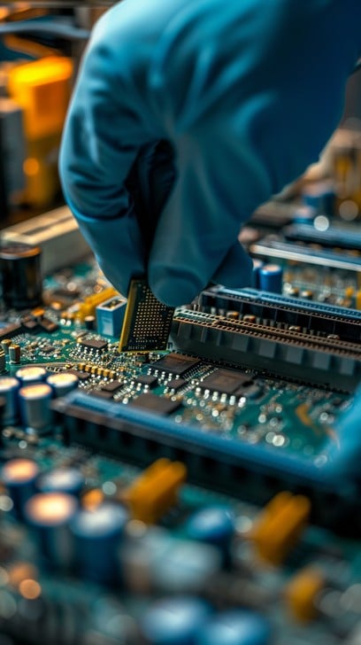
In the semiconductor industry, the journey from an innovative design to a successful product does not end with fabrication. Once a chip is manufactured, it must undergo rigorous testing and specialized packaging before it is ready to power real-world applications. These final steps—though often underestimated—are among the most critical for ensuring functionality, reliability, and market success. At our company, headquartered in Iran with a branch in China, we act as a strategic bridge between local innovation and global execution. We serve a growing network of Iranian customers who rely on us for chip design and manufacturing, and after fabrication, we collaborate with specialized Chinese partners to handle testing and packaging. This combination allows us to deliver complete, end-to-end solutions to our clients at competitive costs and world-class quality standards.
The Importance of Chip Testing
Every semiconductor device must pass through stringent testing
phases to ensure it meets the required standards. Without
proper testing, even the most advanced design can fail in the
market. Testing validates:
• Functionality: Does the chip perform as intended across all
operations?
• Performance: Does it meet specifications for speed, power,
and efficiency?
• Reliability: Can it withstand varying environmental and
workload conditions?
• Yield: How many manufactured chips meet quality
requirements?
Testing is typically divided into two major phases:
Wafer-Level Testing (Wafer Sort):Conducted before
dicing, this process identifies defective dies early, reducing
costs in later stages.
Final Testing (Package Test): Performed after
packaging, this ensures the chip meets performance and
reliability requirements under real conditions.
By
working with Chinese testing facilities, we can guarantee that
our customers’ chips undergo world-class evaluation using
state-of-the-art Automatic Test Equipment (ATE).
The Role of Packaging in Chip Success
Packaging is not just about encasing a chip; it is about enabling its performance and integration into larger systems. The right packaging determines how efficiently a chip can connect, dissipate heat, and withstand physical stress. Key packaging techniques include:

Wire Bonding
A cost-effective solution for many applications.
01
Flip-Chip Packaging
High-performance interconnections for advanced chips.
02
System-in-Package (SiP)
Integration of multiple components into one compact module.
03
3D Packaging
For high-density, next-generation designs.
04
Our collaboration with Chinese packaging houses ensures that we can offer a wide range of packaging technologies tailored to the needs of each client—whether it’s for low-cost IoT devices, high-performance AI processors, or rugged industrial chips.
Our Unique Position: Local Network, Global
Execution
What sets us apart is our dual-market advantage.
Network of Domestic Customers in Iran:
We work with startups, enterprises, and research institutions
in Iran that need reliable chip design, prototyping, and
manufacturing services. Once the chips are fabricated, they
turn to us for the critical testing and packaging stage, which
is essential for their products to succeed in competitive
markets.
Collaboration with Chinese Partners:
Through our China branch, we have access to specialized
testing labs and packaging foundries. These facilities use
cutting-edge tools and processes, ensuring that our clients’
chips meet international benchmarks.
Bridge Between Two Markets:
By combining domestic design and customer demand with
international testing and packaging capacity, we have built a
unique, integrated service chain. This makes us a strong
partner for both Iranian clients and Chinese collaborators.
Workflow: From Fabrication to Packaged Chips:
When a client entrusts us with their project, here’s how the
testing and packaging workflow typically unfolds:
• Fabrication Complete: Chips are produced by our
partner foundries.
• Initial Quality Control: Early inspections ensure
wafers are ready for testing.
• Wafer-Level Testing: Defective dies are identified
and excluded.
• Dicing: Wafers are cut into individual dies.
• Packaging: Dies are packaged using the appropriate
technology for the application.
• Final Testing: Packaged chips are tested under
simulated real-world conditions.
• Delivery to Client: Fully tested and packaged chips
are sent back to our clients in Iran, ready for integration
into their products.
This end-to-end process ensures that our clients not only
receive fabricated chips but also market-ready components.
Industries We Support
Our chip prototyping and manufacturing services serve a wide range of industries:
Artificial Intelligence (AI)
Chips for neural networks and accelerators.
Internet of Things (IoT)
Low-power, compact devices.
Automotive
Chips designed for ADAS and EVs.
Telecommunications
High-speed processors and communication modules.
Industrial Automation
Reliable chips for robotics and control systems.
Healthcare
Chips for wearable and diagnostic devices.
Why us?
Imagine a research institute in Iran developing a new processor for machine learning applications. Our team helps with design and coordination of fabrication. Once the chips are produced, we send them to our Chinese testing and packaging partners. The chips undergo wafer sort, dicing, packaging, and final testing. The packaged chips return to Iran, ready for deployment in the institute’s systems. This smooth pipeline illustrates the value of our cross-border model: Iranian customers get global-quality results, while Chinese companies benefit from a steady flow of business.
In today’s competitive semiconductor landscape, no company can succeed in isolation. The strength lies in partnerships that combine design, manufacturing, testing, and packaging into a seamless ecosystem. Our company is proud to stand at this intersection: Serving Iranian customers with reliable access to global capabilities. Collaborating with Chinese companies for world-class testing and packaging. Acting as a trusted bridge that transforms ideas into market-ready semiconductor solutions. By working with us, clients gain more than a service—they gain a partner dedicated to their success, from the very first design concept to the final packaged chip. Together, we ensure that every chip we deliver is not only designed smartly and manufactured efficiently but also tested rigorously and packaged perfectly for the global market.
