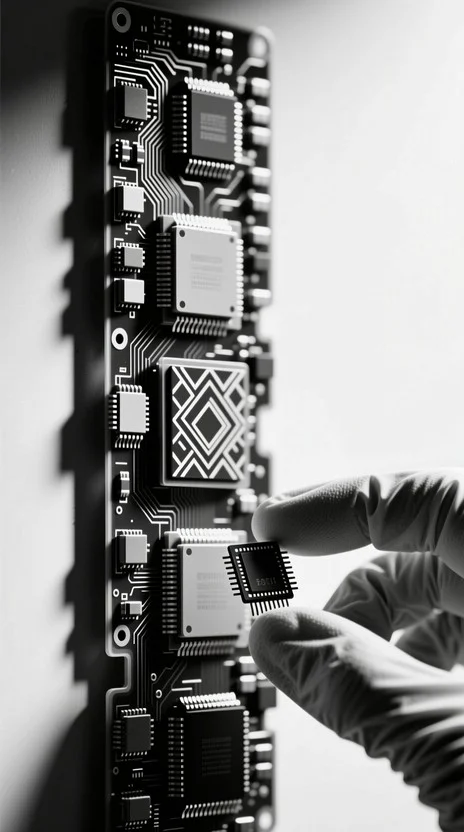
Chip Design & Engineering Services
RayaTech provides integrated chip design and engineering services covering the full spectrum of integrated circuit development, from system-level architecture to tape-out preparation. Our design activities include analog, digital, mixed-signal, RF, and application-specific integrated circuits (ASICs), with a focus on research-driven and application-oriented projects. We work closely with academic groups, research institutes, and technology companies to translate functional specifications into manufacturable circuit designs aligned with target process technologies. Our engineering workflow encompasses circuit design, simulation, verification, and physical implementation using industry-standard EDA tools and validated design methodologies. This includes front-end design, RTL development, analog and RF circuit implementation, layout design, design-for-testability (DFT) considerations, and design rule verification (DRC/LVS). We support multiple technology nodes and process platforms and provide technical guidance on process selection, IP integration, and packaging constraints to ensure manufacturability and scalability. By leveraging a network of experienced local designers and international collaborators, RayaTech acts as a technical interface between system developers and semiconductor manufacturing partners. This approach enables efficient collaboration across design, fabrication, and testing stages while maintaining technical consistency and documentation throughout the development cycle.
Fabless Prototyping & Fabrication Access
RayaTech provides fabless prototyping and fabrication access services to support research and industrial projects requiring semiconductor manufacturing without in-house fabrication facilities. We facilitate access to multi-project wafer (MPW) and single-project wafer (SPW) fabrication runs across a range of silicon and compound semiconductor technologies. These services enable customers to prototype and validate integrated circuit designs with reduced cost, shortened development cycles, and scalable pathways toward volume production. Our team supports customers throughout the pre-fabrication process, including design readiness assessment, process technology selection, tape-out preparation, and coordination with foundry partners. We also provide guidance on packaging options, test planning, and post-fabrication evaluation workflows to ensure alignment between design intent and manufacturing constraints. This integrated approach allows academic and industrial users to move efficiently from design to silicon while maintaining traceability and technical documentation. By operating as a technical liaison between local design teams and international fabrication partners, RayaTech enables reliable and structured access to global semiconductor manufacturing ecosystems. This model supports collaborative prototyping for universities, research centers, and technology companies seeking to validate novel devices, circuits, or system concepts without direct access to foundry infrastructure.

Testing, Packaging & Characterization
RayaTech provides coordinated access to semiconductor testing, packaging, and characterization services to support the full post-fabrication lifecycle of integrated circuits. These services are intended for research institutions and technology companies that require structured validation of fabricated prototypes, from wafer-level testing to packaged device evaluation. Our role is to facilitate technical workflows, documentation, and collaboration with qualified test and assembly partners. We support wafer-level probing, packaged device testing, and electrical characterization under controlled environmental conditions, including voltage, frequency, and temperature variations. Characterization activities include parametric measurements, performance benchmarking, and statistical data analysis to assess compliance with design specifications and technology process limits. Where required, failure analysis workflows and iterative feedback to design teams are coordinated to support design refinement and tape-out iterations. Packaging services include access to standard and advanced packaging technologies, such as wire-bond, flip-chip, and wafer-level packaging, as well as system-in-package configurations. RayaTech acts as a technical interface between design teams and international assembly and test providers, ensuring traceability, process alignment, and delivery of technical reports. This structured approach enables customers to transition from prototype silicon to validated devices suitable for research, pilot production, or system-level integration.

IP Commercialization & Technology Transfer
RayaTech supports the commercialization and transfer of intellectual property (IP) in the semiconductor and electronic systems domains by providing structured pathways from research outcomes to industrial deployment. Our services focus on facilitating the translation of academic and industrial innovations—such as IC designs, process know-how, and system-level technologies—into transferable assets suitable for licensing, joint development, or industrial integration. We provide technical and techno-economic assessment of IP assets, including technology readiness evaluation, manufacturability analysis, and alignment with industry standards and fabrication constraints. This enables technology owners to position their IP for adoption by semiconductor companies, system integrators, and research-driven enterprises. We also assist in defining appropriate commercialization models, including licensing frameworks, collaborative development agreements, and joint ventures. RayaTech acts as a technical and organizational interface between technology developers and industrial stakeholders. Leveraging our presence in Iran and China and our network of academic and industrial partners, we facilitate technical documentation, knowledge transfer workflows, and engagement with fabrication, testing, and system integration partners. This approach supports efficient and traceable technology transfer from laboratory-scale innovation to practical industrial and commercial applications.

International Partnerships
RayaTech develops and manages international partnerships to support semiconductor design, prototyping, testing, and technology deployment across academic and industrial ecosystems. Through structured collaboration frameworks, we connect research institutions, design teams, and technology companies with fabrication, packaging, and system integration partners in East Asia and other global regions. These partnerships are designed to enable efficient access to advanced semiconductor infrastructure and expertise while maintaining clear technical and operational coordination. Our international collaboration model covers technical liaison, project coordination, and joint development activities. We facilitate communication between local design teams and foreign foundries, test houses, and system integrators, ensuring that technical specifications, documentation, and process requirements are aligned across stakeholders. This approach reduces barriers related to geographical separation, process differences, and language or documentation standards. By maintaining an active presence in both domestic and international semiconductor ecosystems, RayaTech serves as a technical interface for cross-border projects. We support collaborative R&D initiatives, technology co-development, and industrial partnerships that require coordinated design, fabrication, and validation workflows. This framework enables research-driven organizations and technology companies to engage in international semiconductor projects with structured technical oversight and traceable collaboration processes.